Forging India’s Silicon Future: How IIT Delhi Is Building the Fabless Chip Ecosystem
For decades, India’s semiconductor story has been framed as one of missed opportunity. The country produces some of the world’s finest chip designers, yet almost all of them work for foreign companies, designing chips that are manufactured abroad and sold back to India. That narrative is being rewritten. At the heart of this transformation is a quiet but determined collaboration between IIT Delhi, industry leaders, and the government—a partnership that is building the infrastructure for India’s fabless chip-design startup ecosystem from the ground up.
A Roadmap for Global Competitiveness
On July 31, 2026, the India Cellular and Electronics Association (ICEA), in collaboration with FITT-IIT Delhi, convened the second India Fabless Semiconductor Design Acceleration Workshop at IIT Delhi. The gathering brought together senior leaders from government, industry, academia, venture capital, and the startup ecosystem to accelerate India’s transition into a global semiconductor product nation.
The roadmap that emerged from these deliberations identified priority chip products, stronger intellectual property (IP) creation, startup support, and easier access to capital as key focus areas under the government’s Semicon 2.0 programme. Electronics and IT Secretary S. Krishnan articulated the ambition clearly: “We must ensure that India’s semiconductor capabilities translate into products designed, owned, and commercialised from India, positioning the country as a leading global semiconductor product nation”.
The Fabless Advantage
The strategic logic behind the fabless push is compelling. Semiconductor chip design is the main value driver, contributing up to 50% of value addition and 30–35% of global semiconductor sales via the fabless segment. Unlike capital-intensive fabrication plants that require investments of ₹40,000–60,000 crore, fabless design companies can be built with relatively modest capital expenditure while generating high value addition.
India Semiconductor Mission CEO Amitesh Kumar Sinha highlighted India’s unique advantage: “Nearly 50 percent of the semiconductor value chain is in design, and around 20 percent of the world’s semiconductor design workforce is Indian. If we provide the right support, these engineers can build product companies in India”.
The IIT Delhi–Cadence Innovation Lab
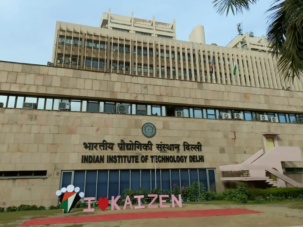
A cornerstone of this ecosystem-building effort is the IIT Delhi–Cadence Innovation Lab, launched in June 2026. The multidisciplinary centre of excellence equips students, researchers, and early-stage startups with access to more than 200 Cadence EDA tools used by the global semiconductor industry.
The lab introduces an Early Master’s Research pathway for selected fourth-year students from IITs and NITs, and supports pre-seed semiconductor startups through an incubator programme offering a lower-cost route to first tape-out. As Cadence CVP Alok Jain noted, students will now use “the same AI-enabled tools they’ll see on day one in industry, closing the gap from classroom to tapeout”. The initiative aligns with the India Semiconductor Mission and the government’s Design Linked Incentive scheme.
A 24-Month Incubation Programme for Fabless Startups
In August 2025, FITT IIT Delhi and AIC IIT Delhi Sonipat, in partnership with Cadence, launched a 24-month incubation programme to groom fabless semiconductor startups in chip design, IP, EDA innovations, and edge-AI hardware. The programme offers startups access to Cadence’s EDA tools, IIT Delhi’s labs and prototyping facilities, technical and business mentorship, investor connects, legal/IP support, and milestone-based grants.
A national selection process shortlists 15–20 teams for a bootcamp, with up to two ventures taken forward for full incubation. The focus areas include fabless SoCs, NPUs and AI accelerators, RISC-V, AI-driven design tools, supply-chain intelligence, and energy-efficient design workflows. FITT MD Dr. Nikhil Agarwal captured the mission succinctly: “India is at a pivotal moment in semiconductors. This program provides the missing bridge—from brilliant design talent to globally competitive deep tech companies”.
Bharat Byte: Scaling the Pipeline
In October 2025, IIT Delhi inaugurated ‘Bharat Byte’ at Technopark in Rai, Sonepat, a strategic initiative to build a strong pipeline of deep-tech startups and innovators in semiconductor and advanced technology domains. Conceived under the guidance of Dr Nikhil Agarwal, the programme seeks to accelerate India’s contribution to the global chip and semiconductor landscape, aligning with the Prime Minister’s vision that “Oil was black gold, but chips are digital diamonds”.
Selected startups receive a grant of ₹10 lakh each and two years of free incubation at AIC Sonepat, along with technical mentorship and infrastructure support from IIT Delhi and Cadence. Dr Agarwal described Bharat Byte as “a national movement to empower innovators and entrepreneurs to develop technologies that will shape India’s digital future”.
The Semicon 2.0 Policy Framework
These institutional efforts are supported by a comprehensive policy framework. The Semicon 2.0 programme, approved with a ₹1.27 lakh crore outlay, represents a strategic pivot from the first phase. Unlike the earlier focus primarily on fabrication plants, Semicon 2.0 aims to build a complete chip ecosystem, with a sharper focus on fabless design companies, specialty chemicals, equipment makers, and talent development.
The expanded framework enables startups, established companies, overseas collaborators, and investors to participate in building India’s semiconductor capabilities. The government’s target of supporting 100 fabless semiconductor companies under Semicon 2.0 is seen as achievable—24 have already received approval. The India Semiconductor Mission is supporting startups through financial assistance, EDA tools, infrastructure, intellectual property support, and by facilitating chip tape-outs.
The Startup Ecosystem Takes Shape
The results of these efforts are becoming visible. Fabless semiconductor startups across India are raising capital and moving from design to pilot production. BigEndian Semiconductors raised $6 million to build secure, high-performance SoCs designed in India for global applications. Vervesemi raised $10 million in Series A for ML-enabled analogue semiconductor solutions. HrdWyr raised $13 million in Series A for product development and market expansion. Mindgrove is gearing up for commercial deployment of its RISC-V-powered Secure IoT chip. At the Bharat Innovates 2026 summit, seven fabless semiconductor-design startups exhibited under the event’s dedicated “Semiconductors” pillar, including Netrasemi, the Thiruvananthapuram-based startup backed by Zoho and Unicorn India Ventures with around ₹125 crore raised to date.
The Road Ahead
The partnership between IIT Delhi and industry leaders represents a fundamental shift in India’s approach to semiconductors. The country is moving from being a source of talent for foreign chip companies to becoming a creator of indigenous semiconductor products. As ICEA Chairman Pankaj Mohindroo noted, “The next phase must focus on creating Indian-owned semiconductor products, IP and globally competitive technology companies”.
With Semicon 2.0 providing the policy framework, IIT Delhi and Cadence providing the infrastructure and mentorship, and a growing pipeline of fabless startups providing the commercial energy, India is building the foundation for what could become a globally competitive semiconductor product nation. The chips that power India’s digital future may soon be designed, owned, and commercialised from India—a transformation that begins in the labs and incubators of IIT Delhi.